
Written by Senior Applications Engineer, Colby Hobart
Rogers Corporation’s latest low-loss RF material, Radix™, does not follow the traditional suite of the materials they sell in this class. Instead of being sold in fully cured, laminated sheet form and pre-metallized for subtractive PCB processing, this material is shipped as an uncured resin, with loaded additives to create the desired RF properties of a 2.8 dielectric constant and a 0.0043 dielectric loss tangent as measured at 10GHz, all while being 3D printable. Due to the high viscosity of this loaded photo-curable polymer and the tendency of the filler material to settle in the liquid resin, Fortify’s 3D print solution, Flux Core, is the only 3D printer on the market capable of printing this low-loss resin and can do so to high print resolution.
With the maturation of this printing process and several pure dielectric applications advancing to the commercial level, metallized parts are in the pipeline right behind these bare dielectrics. Fortify has partnered with Averatek to explore metallized parts and has performed several studies on the metallization of Radix material with very good results. With metallized parts, comes another portion of insertion loss on the device beyond just the dielectric loss of the material. Metal conductivity is the main driver of the ohmic portion of insertion loss. Averatek is capable of achieving near the conductivity of bulk copper with their copper deposition. This process is performed with traditional plating, using a proprietary selective seed layer, traditional electroless copper that becomes selective due to the seed, and electroplated copper to achieve traditional signal thicknesses, such as 1/4oz, 1/2oz, or 1oz copper, or thicker upon request. Surface roughness of the signal metal as facing the ground plane(s) of the transmission line is also a major driver of insertion loss. The first five skin depths of the copper against the laminate and how rough that copper is will play a role in insertion loss. Copper roughness is typically specified as Ra (absolute value of the average peak or valley height relative to the arithmetic mean of the roughness), Rz (highest peak – lowest valley), or Rq (RMS value of the peak and valley roughness). However, there is an additional parameter of importance. The periodicity of the roughness also plays a substantial role in how much the copper roughness affects insertion loss. The more stretched out the peaks and valleys of the roughness are, the less impact they will have on insertion loss as compared to perfectly smooth copper. The first step in characterizing the copper roughness as applied by Averatek to the 3D printed polymers from Fortify is to create simple transmission lines to characterize over frequency on a network analyzer. Microstrip structures were chosen for this purpose as a simple transmission line. The copper roughness to be characterized here will be mainly the copper surface facing inward to the dielectric. Since the copper is an additive process, it is expected that the roughness of the copper will be dictated by the roughness of the dielectric face that the copper is applied.
An experiment was designed to determine the impact of insertion loss of the available stock surface roughnesses that could occur on different faces of a device as printed on a Flux Core machine at Fortify. Using a default build plate, eight print orientations were selected that would produce unique roughness profiles on the signal side of a microstrip device. For each orientation, a 2” long structure and an 8” long structure were printed. These orientations included three varieties where the microstrip substrates were printed parallel to the build plate – signal side directly on the build plate, signal side directly on the reservoir film, and signal side directly on the film with ground side offset from the build plate by printed support structures. The last variety was added to control the thickness variation of the substrate. Five additional varieties were printed with the signal side of the substrate perpendicular to the build plate. The angle of the device pairs was varied from horizontal along the build plate (0°) to a full vertical span from the build plate (90°) and three additional angles in between (30°, 40°, and 70°). A photo showing many of these orientations, along with the printed support structures to stabilize them, is shown in Figure 1.

Figure 1: Build Plate Containing Several Varieties Microstrip Dielectrics
All samples were then characterized for surface roughness using Fortify’s Keyence One-Shot 3D VR laser profilometry system. Three areas along the surface of each device were measured and averaged. The average roughnesses for the 8 styles of the device were then recorded before shipping them out for metallization. Table 1 and Table 2 illustrate these results.

Table 1: Surface Roughness Reported as Ra for Circuit Dielectrics Printed Parallel to the Build Plate

Table 2: Surface Roughness Reported as Ra for Circuit Dielectrics Printed Perpendicular to the Build Plate
Averatek performed metallization of the circuits according to two artwork varieties based on some variation of nominal thickness due to print orientation. The two artwork ensured that a 50 +/- 2 ohm characteristic impedance was maintained across all devices. Figure 2 shows an example of a metallized device.
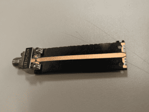
Figure 2: Example of a Metallized 2” Microstrip Circuit Backside Groundplane Fully Metallized
All circuits were then characterized using an Intercontinental Microwave W7000 fixture that uses two built-in probes to contact the microstrip line and interfaces the device with a Keysight N5230 PNA-L network analyzer. All circuits were swept from 50MHz to 20GHz and S-parameters for all measurements were exported as .csv files in magnitude/phase format. In order to de-embed the effects of the fixture and launch points of the microstrip devices, the S21 insertion loss magnitude results of the 2” circuit for each orientation pair were subtracted from the S21 magnitude results of the the 8” circuit of the same orientation. The resulting value was then divided by the remaining 6” of the device and plotted to show the insertion loss per inch over the frequency of each of the print orientations. Results are shown below in Figure 3 and Figure 4.

Figure 3: Insertion Loss per Inch for Three Parallel-to-Plate Varieties of Microstrip Circuits

Figure 4: Insertion Loss per Inch of Five Perpendicular-to-Plate Varieties of Microstrip Circuits
Since the devices were swept broadband and the response appears to be quite linear with respect to frequency and taking into account that the effect of VSWR becomes greater with frequency, it is pertinent to discuss the results at center band of the sweep for a final comparison, as a broadband comparison will become quite complex. In order to determine the insertion loss value at 10GHz, due to local insertion loss variation from measurement tolerance and VSWR, the loss/inch data was averaged over a 3GHz span centered around the center frequency of the sweep. There was one trace with more erratic results from some fabrication or measurement anomaly, so to not be biased as much by its behavior away from center band, it was averaged over a 1GHz span. That trace is the 0 deg perpendicular variety and the result should be considered less accurate than the rest. All results of this analysis are shown in Table 3.

The supported structure stands out as an outlier at 0.28dB per inch and it is worth noting that this print may be affected by the bumps left behind by the printed support structures on the ground side suggesting that there is a repeatedly wavering characteristic impedance along the length of the device. This likely caused some extra variation in VSWR that could contribute to some excess loss. So, for the purpose of the final comparison, the validated insertion loss of the experiment should be considered as 0.21dB per inch to 0.25dB per inch at 10GHz. Considering that the surface roughness across the experiment was measured to be sub 1um to almost 10um, this variation in insertion loss is much lower than expected, almost considered negligible. As far as comparison to traditional electrodeposited foils, this magnitude of roughness variation would be expected to induce a much larger range in insertion loss. The reasoning for the small effect on insertion loss range lies in the periodicity of the roughness applied. Because both the roughness induced by the build plate and that created by the 75um-spaced layer lines create peaks and valleys that are spaced apart by large distances relative to the roughness observed on standard electrodeposited and treated foils, the extra insertion loss due to this widely spaced roughness becomes very small. It is noted that this experiment used 30MIL thick dielectrics due to the limitations of feature sizes that could reliably print across all orientations. To increase the effect of the copper roughness on the loss measurement a narrower transmission line could be used. This would help isolate the effect of the copper roughness. To achieve this, a thinner dielectric test could help show the minor differences in effect of roughness. However, the practical circuit designer would seek out a thicker dielectric as it fits within the design guidelines of the project and a 30MIL dielectric is reasonable for most application spaces. This experiment shows that for a reasonable, average dielectric thickness that the insertion loss per inch on Radix materials as printed on Fortify Flux Core printer does not change enough for high concern on orientation of parts and that all sides of a printed part can be utilized for metallization.